- 您现在的位置:买卖IC网 > Sheet目录317 > C8051T610DB24 (Silicon Laboratories Inc)DAUGHTER BOARD T610 24QFN SOCKET
�� �
�
�C8051T610/1/2/3/4/5/6/7�
�8.1.� Output� Code� Formatting�
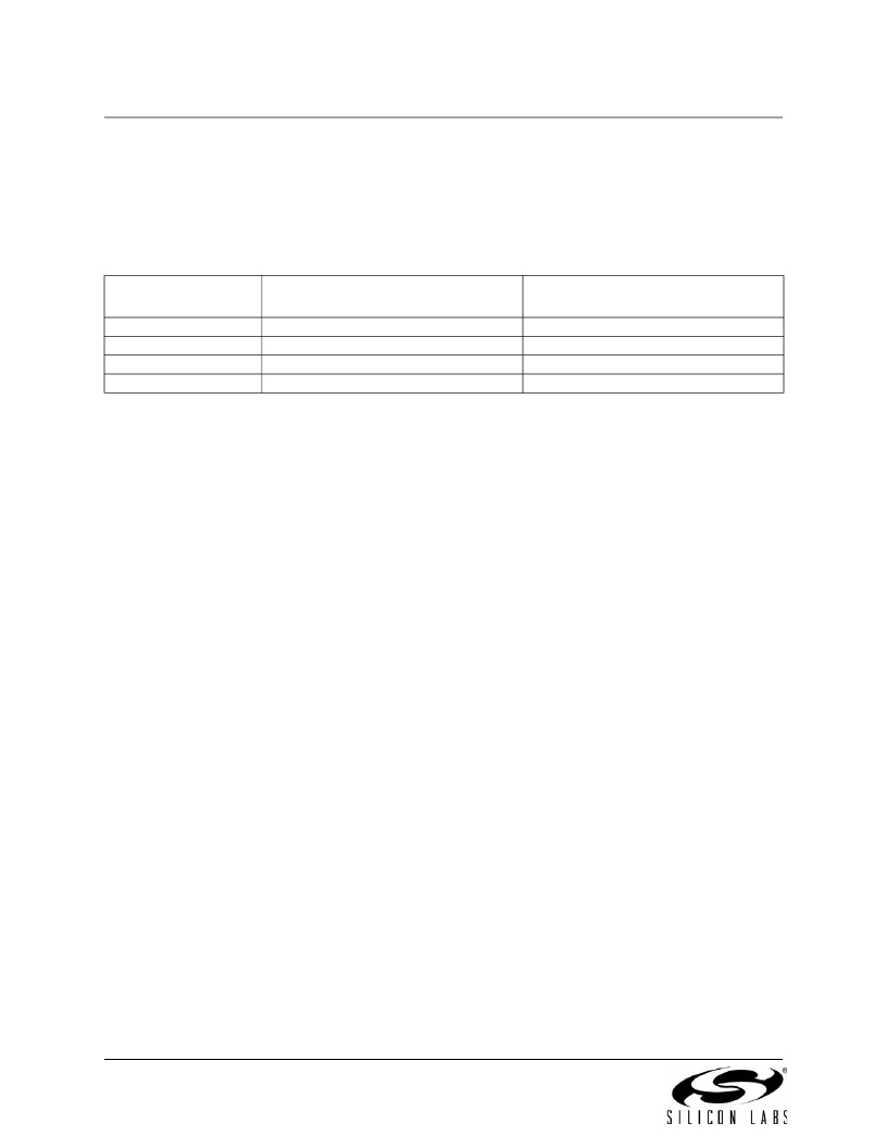
�The� ADC� measures� the� input� voltage� with� reference� to� GND.� The� registers� ADC0H� and� ADC0L� contain� the�
�high� and� low� bytes� of� the� output� conversion� code� from� the� ADC� at� the� completion� of� each� conversion.� Data�
�can� be� right-justified� or� left-justified,� depending� on� the� setting� of� the� AD0LJST� bit.� Conversion� codes� are�
�represented� as� 10-bit� unsigned� integers.� Inputs� are� measured� from� 0� to� VREF� x� 1023/1024.� Example�
�codes� are� shown� below� for� both� right-justified� and� left-justified� data.� Unused� bits� in� the� ADC0H� and� ADC0L�
�registers� are� set� to� 0.�
�Input� Voltage�
�VREF� x� 1023/1024�
�VREF� x� 512/1024�
�VREF� x� 256/1024�
�0�
�Right-Justified� ADC0H:ADC0L�
�(AD0LJST� =� 0)�
�0x03FF�
�0x0200�
�0x0100�
�0x0000�
�Left-Justified� ADC0H:ADC0L�
�(AD0LJST� =� 1)�
�0xFFC0�
�0x8000�
�0x4000�
�0x0000�
�8.2.� 8-Bit� Mode�
�Setting� the� ADC08BE� bit� in� register� ADC0CF� to� 1� will� put� the� ADC� in� 8-bit� mode.� In� 8-bit� mode,� only� the� 8�
�MSBs� of� data� are� converted,� and� the� ADC0H� register� holds� the� results.� The� AD0LJST� bit� is� ignored� for� 8-�
�bit� mode.� 8-bit� conversions� take� two� fewer� SAR� clock� cycles� than� 10-bit� conversions,� so� the� conversion� is�
�completed� faster,� and� a� 500� ksps� sampling� rate� can� be� achieved� with� a� slower� SAR� clock.�
�8.3.� Modes� of� Operation�
�ADC0� has� a� maximum� conversion� speed� of� 500� ksps.� The� ADC0� conversion� clock� is� a� divided� version� of�
�the� system� clock,� determined� by� the� AD0SC� bits� in� the� ADC0CF� register.�
�8.3.1.� Starting� a� Conversion�
�A� conversion� can� be� initiated� in� one� of� six� ways,� depending� on� the� programmed� states� of� the� ADC0� Start� of�
�Conversion� Mode� bits� (AD0CM2� –� 0)� in� register� ADC0CN.� Conversions� may� be� initiated� by� one� of� the� fol-�
�lowing:�
�1.� Writing� a� 1� to� the� AD0BUSY� bit� of� register� ADC0CN�
�2.� A� Timer� 0� overflow� (i.e.,� timed� continuous� conversions)�
�3.� A� Timer� 2� overflow�
�4.� A� Timer� 1� overflow�
�5.� A� rising� edge� on� the� CNVSTR� input� signal�
�6.� A� Timer� 3� overflow�
�Writing� a� 1� to� AD0BUSY� provides� software� control� of� ADC0� whereby� conversions� are� performed� "on-�
�demand".� During� conversion,� the� AD0BUSY� bit� is� set� to� logic� 1� and� reset� to� logic� 0� when� the� conversion� is�
�complete.� The� falling� edge� of� AD0BUSY� triggers� an� interrupt� (when� enabled)� and� sets� the� ADC0� interrupt�
�flag� (AD0INT).� Note:� When� polling� for� ADC� conversion� completions,� the� ADC0� interrupt� flag� (AD0INT)�
�should� be� used.� Converted� data� is� available� in� the� ADC0� data� registers,� ADC0H:ADC0L,� when� bit� AD0INT�
�is� logic� 1.� Note� that� when� Timer� 2� or� Timer� 3� overflows� are� used� as� the� conversion� source,� Low� Byte� over-�
�flows� are� used� if� Timer� 2/3� is� in� 8-bit� mode;� High� byte� overflows� are� used� if� Timer� 2/3� is� in� 16-bit� mode.�
�See� Section� “25.� Timers”� on� page� 170� for� timer� configuration.�
�Important� Note� About� Using� CNVSTR:� The� CNVSTR� input� pin� also� functions� as� a� Port� I/O� pin.� When� the�
�CNVSTR� input� is� used� as� the� ADC0� conversion� source,� the� associated� pin� should� be� skipped� by� the� Digi-�
�tal� Crossbar.� See� Section� “21.� Port� Input/Output”� on� page� 113� for� details� on� Port� I/O� configuration.�
�40�
�Rev� 1.1�
�发布紧急采购,3分钟左右您将得到回复。
相关PDF资料
C8051T630DB20
BOARD SOCKET DAUGHTER 20-QFN
CAN-100
BOARD EVAL RS232 100QFP
CANADAPT28
KIT ADAPTER CANDEMOBOARD 28PLCC
CAT24AA01WI-GT3
IC EEPROM SERIAL 1KB I2C 8SOIC
CAT24AA02WI-G
IC EEPROM SERIAL 2KB I2C 8SOIC
CAT24C01ZI-G
IC EEPROM SERIAL 1KB I2C 8MSOP
CAT24C03WI-G
IC EEPROM SERIAL 2KB I2C 8SOIC
CAT24C04ZI-G
IC EEPROM SERIAL 4KB I2C 8MSOP
相关代理商/技术参数
C8051T610DB28
功能描述:子卡和OEM板 C8051T610 Family Socket Daughtr Board RoHS:否 制造商:BeagleBoard by CircuitCo 产品:BeagleBone LCD4 Boards 用于:BeagleBone - BB-Bone - Open Source Development Kit
C8051T610DB32
功能描述:子卡和OEM板 C8051T610 Family Socket Daughtr Board RoHS:否 制造商:BeagleBoard by CircuitCo 产品:BeagleBone LCD4 Boards 用于:BeagleBone - BB-Bone - Open Source Development Kit
C8051T610DK
功能描述:开发板和工具包 - 8051 C8051T610 Series Development Kit RoHS:否 制造商:Silicon Labs 产品:Development Kits 工具用于评估:C8051F960, Si7005 核心: 接口类型:USB 工作电源电压:
C8051T610-GQ
功能描述:8位微控制器 -MCU 16KB 10ADC 32Pin MCU RoHS:否 制造商:Silicon Labs 核心:8051 处理器系列:C8051F39x 数据总线宽度:8 bit 最大时钟频率:50 MHz 程序存储器大小:16 KB 数据 RAM 大小:1 KB 片上 ADC:Yes 工作电源电压:1.8 V to 3.6 V 工作温度范围:- 40 C to + 105 C 封装 / 箱体:QFN-20 安装风格:SMD/SMT
C8051T610-GQR
功能描述:8位微控制器 -MCU 16KB 10ADC 32Pin MCU RoHS:否 制造商:Silicon Labs 核心:8051 处理器系列:C8051F39x 数据总线宽度:8 bit 最大时钟频率:50 MHz 程序存储器大小:16 KB 数据 RAM 大小:1 KB 片上 ADC:Yes 工作电源电压:1.8 V to 3.6 V 工作温度范围:- 40 C to + 105 C 封装 / 箱体:QFN-20 安装风格:SMD/SMT
C8051T611-GM
功能描述:8位微控制器 -MCU 16KB 10ADC 28Pin MCU RoHS:否 制造商:Silicon Labs 核心:8051 处理器系列:C8051F39x 数据总线宽度:8 bit 最大时钟频率:50 MHz 程序存储器大小:16 KB 数据 RAM 大小:1 KB 片上 ADC:Yes 工作电源电压:1.8 V to 3.6 V 工作温度范围:- 40 C to + 105 C 封装 / 箱体:QFN-20 安装风格:SMD/SMT
C8051T611-GMR
功能描述:8位微控制器 -MCU 16KB 10ADC 28Pin MCU RoHS:否 制造商:Silicon Labs 核心:8051 处理器系列:C8051F39x 数据总线宽度:8 bit 最大时钟频率:50 MHz 程序存储器大小:16 KB 数据 RAM 大小:1 KB 片上 ADC:Yes 工作电源电压:1.8 V to 3.6 V 工作温度范围:- 40 C to + 105 C 封装 / 箱体:QFN-20 安装风格:SMD/SMT
C8051T612-GQ
功能描述:8位微控制器 -MCU 8KB 10ADC 32Pin MCU RoHS:否 制造商:Silicon Labs 核心:8051 处理器系列:C8051F39x 数据总线宽度:8 bit 最大时钟频率:50 MHz 程序存储器大小:16 KB 数据 RAM 大小:1 KB 片上 ADC:Yes 工作电源电压:1.8 V to 3.6 V 工作温度范围:- 40 C to + 105 C 封装 / 箱体:QFN-20 安装风格:SMD/SMT